SPI Communication
Updated: 12Aug2024 02:22:42 UTC 2024-08-12T02:22:42Z
Rating: (0 reviewsThis article has not been rated yet)
The Serial Peripheral Interface (SPISerial Peripheral Interface) provides full-duplex synchronous serial communication at high speeds over short distances. It is often used for interfacing a microcontroller or SBCSingle Board Computer with peripheral devices such as sensors, ADCAnalog-to-Digital Converter (ADC, A/D, or A-to-D)s, RTCReal-Time Clocks, LCDLiquid Crystal Displays, external memory modules, and wireless transceiver modules.
One benefit of SPI is data can be transferred in a continuous stream without interruption at higher speeds compared to UARTUniversal Asynchronous Receiver-Transmitter and I2CInter-Integrated Circuit. Also referred to as IIC or I2C. where data is sent in packets that are limited to a specific number of bits. SPI also offers full-duplex communication where data can be sent and received at the same time, in contrast to UART and I2C that are half-duplex where data can be only sent or received in one direction at a time.
This introduction to SPI will cover its hardware wiring, data transmission signals, and speed.
Hardware Wiring
SPI provides synchronous full-duplex communication on a point-to-point bus between a master device and a slave device using four lines.
- MOSI (Master Out, Slave In):
- Used by the master to transmit data to the slave.
- MISO (Master In, Slave Out):
- Used by the slave to transmit data to the master.
- SCLK (System Clock):
- Used by the master to transmit the clock signal. Also referred to as SCK, SCL or CLK.
- SS (Slave Select):
- Used by the master to select a slave. Also referred to as CS (Chip Select). The SS or CS is usually active low and may be denoted with an overline (SS or CS).
SPI operates on the master-slave principle with the master as the main controller and peripheral devices as the slaves. Two different wiring configuration can be used for multiple slave devices: the independent slave configuration and daisy chain slave configuration.
In the independent slave configuration, the master uses different SSSlave Select (SS) is the SPI output line from the master device to indicate that data is being sent. Also referred to as Chip Select (CS). lines for each slave device shown in the figure below. When the master wants to communicate with a particular slave, it pulls its SSSlave Select (SS) is the SPI output line from the master device to indicate that data is being sent. Also referred to as Chip Select (CS). state LOW during the duration of the communication exchange.
In the daisy chain slave configuration, the master uses only one SSSlave Select (SS) is the SPI output line from the master device to indicate that data is being sent. Also referred to as Chip Select (CS). line connected to all the slave devices shown in the figure below. When the master wants to communicate with a particular slave, it pulls its SSSlave Select (SS) is the SPI output line from the master device to indicate that data is being sent. Also referred to as Chip Select (CS). state LOW to initiate communication, sends data over its MOSIMaster Out Slave In (MOSI) is the SPI data output line from the master device to the first slave device in the chain, which then flows from one slave to the next in the chain.
Data Transmission
SPI data does not have a standardized packet structure like UART and I2C, rather when the SS line is activated the MOSI/MISO line data is transferred one bit at a time each clock cycle and the meaning of those bits are application specific. However, there are standard modes in SPI that determine when the data is sent and read.
There are four different SPI modes that can be configured in the master device. Each mode depends on the states of the Clock Polarity (CPOL) and Clock Phase (CPHA). The CPOL can be 0 or 1 that determines the clock's idle state as LOW or HIGH, respectively. The CPHA can be 0 or 1 that represents the phase of each data bits transmission cycle relative to SCLK. The different modes and corresponding CPOL and CPHA values that determine when data is sent and read is given in the table below.
| Mode | CPOL | CPHA | Data Out | Data In |
|---|---|---|---|---|
| 0 | 0 | 0 | when SS activates and subsequent falling SCLK | rising SCLK |
| 1 | 0 | 1 | rising SCLK after SS activates | falling SCLK |
| 2 | 1 | 0 | when SS activates and subsequent rising SCLK | falling SCLK |
| 3 | 1 | 1 | falling SCLK after SS activates | rising SCLK |
Bit Ordering
The order in which the bits are transmitted over a communication channel is called Endianness. There are two types of endianness. Little-endian has the Least Significant Bit (LSBThe Least Significant Bit (LSB) in a binary number is the bit that represents the smallest place value carrying the lowest weight. It is also sometimes referred to as the low-order bit or right-most bit due to the convention in positional notation of writing less significant digits further to the right.) sent first and Most Significant Bit (MSBThe Most Significant Bit (MSB) in a binary number is the bit that represents the largest place value carrying the most weight. It is also sometimes referred to as the high-order bit or left-most bit due to the convention in positional notation of writing less significant digits further to the right.) sent last. Big-endian transmits the MSB first and the LSB last.
For example, suppose we want to send the number 45 serially over a transmission line. The number 45 is 00101101 in binary. Big-endian bit ordering would be transmitted left to right (00101101) and little-endian would be transmitted right to left (10110100).
In SPI communication data is usually shifted out of the master and slave devices MSBThe Most Significant Bit (MSB) in a binary number is the bit that represents the largest place value carrying the most weight. It is also sometimes referred to as the high-order bit or left-most bit due to the convention in positional notation of writing less significant digits further to the right. first (Big-endian), although some devices send data out LSBThe Least Significant Bit (LSB) in a binary number is the bit that represents the smallest place value carrying the lowest weight. It is also sometimes referred to as the low-order bit or right-most bit due to the convention in positional notation of writing less significant digits further to the right. first (Little-endian). The bit ordering can be set by the software on the master device. For example, in the Arduino SPI Library, this is controlled by the setBitOrder() function.
Transmission Speed
SPI is the fastest protocol compared to UARTUniversal Asynchronous Receiver-Transmitter and I2CInter-Integrated Circuit. Also referred to as IIC or I2C.. The communication speeds of SPI depend on the clock frequency of the master device using a frequency supported by slaves devices. In SPI each bit is transmitted on a clock edge, therefore the data rate (in bits) is the same as the SPI clock frequency which typically runs at a maximum of half the system clock of the master device.
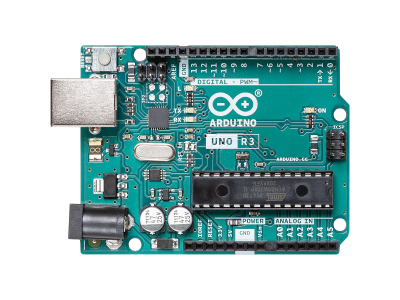
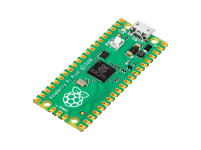
For example, if the master device is an Arduino Uno R3 or Nano microcontroller board with a 16MHz ATmega328P MCUMicrocontroller Unit, the maximum data rate is 8MbpsMegabits per second. If the master device is a RPiRaspberry Pi Pico with a 133MHz RP2040 MCUMicrocontroller Unit, the maximum data rate is 66Mbps. These are the theoretical maximum data rates which does not include any protocol overhead on the bits transmitted (e.g., idle cycles, framing information, parity bits, etc.).
Some slave devices may not be able to handle the maximum SPI clock frequency of the master device. To accommodate lower speeds of slave devices, the SPI clock speed of the master device can be configured in software. For example, in the Arduino SPI Library, the SPI clock speed is set the setClockDivider() function which divides the system clock. On AVR based boards, the dividers available are 2, 4, 8, 16, 32, 64, or 128. The default setting is 4, which sets the SPI clock to one-quarter the frequency of the system clock (e.g., 4MHz for boards with a 16MHz MCUMicrocontroller Unit).
Quad SPI (QSPI)
Quad Serial Peripheral Interface (QSPIQuad Serial Peripheral Interface (QSPI) is a serial communication interface designed for talking to flash chips by using 4 data lines.) is an extension to the standard SPI bus with two additional data lines to improve the throughput four times and is often used on a microcontroller or SBCSingle Board Computer PCBPrinted Circuit Board to communicate with flash memory chips.
Instead of the MOSI and MISO lines in standard SPI, the QSPI data lines are IO0, IO1, IO2, and IO3. While SPI uses Single Data Rate Mode where a data line can change at either the rising or falling edge of the clock, QSPI supports Double Data Rate Mode where a data line can change on both the rising and falling edge of the clock, effectively doubling the speed of transmission.
Conclusion
This introduction to SPI covered its hardware wiring, data transmission signals, and speed. There are advantages and disadvantages to using SPI compared to other wired communication protocols such as UARTUniversal Asynchronous Receiver-Transmitter and I2CInter-Integrated Circuit. Also referred to as IIC or I2C..
Some of the advantages of using SPI are:
- Full-duplex communication (UART and I2C are half-duplex)
- Data can be transferred at higher speeds in a continuous stream without interruption (no start/stop bits or slave addressing)
- Complete flexibility for the bits transferred (data frames are not limited to 9 bit in UART and 8 bit word in I2C)
- Supports multiple slaves
Some of the disadvantages of using SPI are:
- It uses more wires than UART and I2C
- Only can have a single master, whereas I2C is multi-master
- Requires separate SS lines to each slave that can be inconvenient if numerous slaves are used
- No acknowledgment that the data has been successfully received as in I2C
- No message error checking like the parity bit in UART
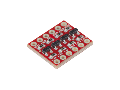
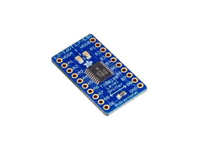
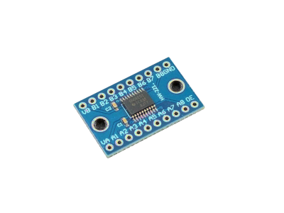
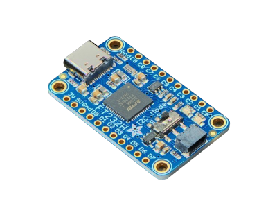
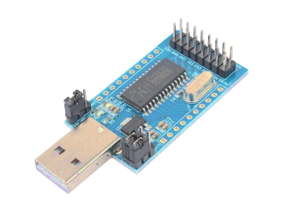
As with UART and I2C, the data lines of SPI between devices should have compatible logic voltage levels (e.g., 3.3V to 3.3V or 5V to 5V). If the devices operate at different voltages without any internal level shifting circuitry built in, then external Logic Level Converter modules such as a BSS138 FETField Effect Transistor or a buffer/driver level shifter ICIntegrated Circuit can be used (a list of options is provided in the Products section).





(0) Comments
Sign in to leave a comment
Sign In