USB Serial Adapters
Updated: 19Aug2024 01:20:24 UTC 2024-08-19T01:20:24Z
Rating: (0 reviewsThis article has not been rated yet)
This article gives an overview of USBUniversal Serial Bus serial adapters specifically for converting USB signals from a computer to/from UARTUniversal Asynchronous Receiver-Transmitter, I2CInter-Integrated Circuit. Also referred to as IIC or I2C., and/or SPISerial Peripheral Interface protocols commonly used with devices such as microcontrollers and sensors. This article will also provide a comparison of different USB serial adapters.
There are many sensors and modules that output digital signals in UART, I2C, and/or SPI. USB Serial Adapters can be used as a computer interface, automatically converting the standard communication signal to the complex USB protocol in order to transfer data to the computer over a USB cable. This is illustrated in the figure below.
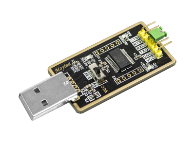
The USB Serial Adapter has a chip that processes the USB signals and applies the correct voltages and timing for the (UART, I2C, SPI) serial output. Adapters can be specifically designed for either 3.3V serial or 5V serial and some can handle both. There are also adapters with a physical switch to manually change between 3.3V and 5V serial. They also usually provide the USB 5V supply as an output to power low current devices.
In order for the computer to detect and process the data, drivers must be installed on the computer. These drivers specify a command set your computer can use to query the chip by creating a virtual COMCommunication port which shows up in Device Manager on Windows, and under /dev on Linux and MacOS. Some chip models, like FTDIFuture Technology Devices International, have drivers installed by default while with some other chip models (e.g., SiLabs CP2102, Prolific PL2303, WCH CH340, etc.) the drivers must be installed manually.
Functional Overview
USB adapters usually have a mid-low class MCUMicrocontroller Unit that provides bi-directional raw buffers of FIFOFirst In First Out types, manages data flow control, the configuration of UART/I2C/SPI, as well as USB descriptors. In many cases the adapter may provide other options as ADCAnalog-to-Digital Converter (ADC, A/D, or A-to-D)/DACDigital-to-Analog Converter (DAC, D/A, or D-to-A) and few GPIOGeneral Purpose Input Outputs that typically come with an MCU. The main functional hardware blocks that make up a typical USB adapter are illustrated in the figure below.
- USB Transceiver:
- Provides the USB electrical requirements over D+ (DP) and D- (DM) wires and the physical interface to the USB cable for the USB protocol.
- USB Serial Interface Engine (SIESerial Interface Engine):
- Performs the processing of the USB signals: the parallel to serial and serial to parallel conversion of the USB data, and outputs to USB transceiver to generate the external USB D+ and D- signals timing. In accordance with the USB specification, it performs bit stuffing/un-stuffing, packet formation including encoding and decoding, SYNC and EOP frame signal, and CRCCyclic Redundancy Check generation (and also checks the CRC on the USB data stream).
- Memory:
- Typically an EEPROMElectrically Erasable Programmable Read-Only Memory that can be programmed by the USB and may be used to customize the USB Vendor ID, Product ID, Product Description String, Power Descriptor, Device Release Number, and Device Serial Number and various other USB configuration descriptors. The adapter is usually supplied with the internal memory pre-programmed.
- Voltage Regulator:
- Adapters include an on-chip voltage regulator, typically 5V to 3.3V/1.8V, allowing the chip configured as either a USB bus-powered device or a USB self-powered device. This is mainly used to create the reference voltage to driving the USB transceiver, but the 3.3V output is sometimes offered to power low current external devices.
- Oscillator Clock:
- The clock generator module generates the reference clock signals for internal chip logic and baud rate generator for UART/I2C/SPI. The oscillator source (crystal, ceramic resonator, etc.) could be internal or external, depending on the device.
- UART/I2C/SPI Controller:
-
This block handles the transfer of data between the FIFOFirst In First Out transmit and receive buffers and
registers, and usually includes a precise baud rate generator set from USB command. It performs asynchronous
7 or 8 bit parallel to serial and serial to parallel conversion of the data for the UART
interface.
If the adapter supports multiple protocols, such as I2C and SPI, the controller usually contains an Multi-Protocol Synchronous Serial Engine (MPSSEMulti-Protocol Synchronous Serial Engine) that can be configured under software command. Control signals supported by UART mode can include RTSReady To Send, CTSClear To Send, DSRData Set Ready, DTRData Transmit Ready, DCDData Carrier Detect and RIRing Indicator. RTS/CTS, DSR/DTR and XON/XOFF handshaking options may also be supported.
Pin Functions
The pins on USB serial adapters usually have power pins and data pins, and sometimes include control pins depending on the devices. Below is a description of common pins found in each of these categories.
Power Pins
- VCCVoltage Collector Collector (VCC) is the supply voltage at the collector of a transistor. The double subscript notation of repeating letters "CC" is used to denote a power supply voltage that is relative to ground. /VDDVoltage Drain Drain (VDD) is the supply voltage at the Drain of a transistor. The double subscript notation of repeating letters "DD" is used to denote a power supply voltage that is relative to ground. :
- Power pin, which can be either 5V / 3.3V. Sometimes there is a 5V / 3.3V jumper or switch on the board that controls the output voltage on the VCCVoltage Collector Collector (VCC) is the supply voltage at the collector of a transistor. The double subscript notation of repeating letters "CC" is used to denote a power supply voltage that is relative to ground. pin.
- GND:
- Ground pin
Data Pins
- TX:
- data transmit pin. This pin sends the serial output.
- RX:
- data receive pin. This pin receives the serial input.
UART
- SDL (Serial Data Line):
- used by the master or slave to transmit/receive data
- SCL (Serial Line Clock):
- used by the master to transmit the clock signal
I2C
- MOSI (Master Out, Slave In):
- used by the slave to transmit data to the master
- MISO (Master In, Slave Out):
- used by the master to transmit the clock signal
- SCLK (System Clock):
- used by the master to transmit the clock signal. Also referred to as SCK, SCL or CLK.
- SS (Slave Select):
- used by the master to select a slave
SPI
Control Pins
For the control pin descriptions given below, the computer is frequently referred to as the Data Terminal Equipment (DTEData Terminal Equipment) and the device (sensor, microcontroller, etc.) as the Data Circuit Terminating Equipment (DCEData Circuit Terminating Equipment or Data Communication Equipment or Data Carrier Equipment. ). The VCCVoltage Collector Collector (VCC) is the supply voltage at the collector of a transistor. The double subscript notation of repeating letters "CC" is used to denote a power supply voltage that is relative to ground. can also be referred to as the Data Communication Equipment or Data Carrier.
- RTS:
- Ready To Send control output. When the DTEData Terminal Equipment (computer) tells the DCEData Circuit Terminating Equipment or Data Communication Equipment or Data Carrier Equipment. (device) of it wants to send data, it is set high, and the request is granted with with CTSClear To Send. When a DTEData Terminal Equipment wants to stop the data sending into it, it sets RTSReady To Send to low meaning "Do not send to me".
- CTS:
- Clear To Send control input (usually active low). This comes from the device to grant the RTS request that data can be sent to the device. The device can also lower CTS when its internal buffer is full.
- DTR:
- Data Transmit Ready output (usually active low) when active the DTE tells the DCE that its ready to communicate. Inactive means the DTE is telling the DCE that its internal buffer is full and not ready to transmit.
- DSR:
- Data Set Ready input (usually active low) when active the DCE tells the DTE that its ready to communicate. Inactive mean tells the DCE no longer listening and so sending any further characters is pointless.
- DCD:
- Data Carrier Detect input that is usually present inside an RS-232 cable. This signal is a high/low status bit whose purpose varies with different devices, but typically indicates that the DCE is receiving a carrier from a remote DCE.
- RI:
- Ring Indicator Control Input. DCE has detected an incoming ring signal on the telephone line. When a remote wake up option is enabled, this can be used to indicate the phone line is still "connected" and receiving a carrier signal from the modem at the other end and resume the PC USB host controller from suspend.
Originally RTS/CTS was for half-duplex modems to coordinate who was sending and who was receiving and wasn't supposed to ever be a flow control mechanism. However, RTS/CTS got misused for flow control so often that it became standard.
When using the serial adapter to program a microcontroller, some boards like the Arduino allow the RTS or DTR pin to auto-reset microcontroller when a new sketch is downloaded without having to hit the reset button on the microcontroller.
I/O Voltage Levels
Communication with UART/I2C/SPI uses two voltage levels to indicate a 0 bit and a 1 bit. The voltage level values depends on the device:
- RS232/RS-422/RS-485 serial uses negative and positive voltages up to -15V and +15V, where the negative voltage level is a logical 1 and the positive voltage is logical 0.
- 5V devices, such as the Arduino Uno, use voltage levels 0V and 5V, where the 0V voltage level is a logical 0 and the 5V voltage is logical 1.
- 3.3V devices, such as the RPiRaspberry Pi Pico, use voltage levels 0V and 3.3V, where the 0V voltage level is a logical 0 and the 3.3V voltage is logical 1.
- 1.8V devices, such as the STM32F048x6 microcontrollers, use 0V and 1.8V, where the 0V voltage level is a logical 0 and the 1.8V voltage is logical 1.
It is important to use the correct voltage to avoid damaging your device. Inserting 15V into a 5V or 3.3V device will damage the device. A 5V device can receive 3.3V, but transmitting 5V to a 3.3V input may cause damage. A 5V to 3.3V logic level converter is useful for ensuring both ends are receiving the right voltages.
UARTUniversal Asynchronous Receiver-Transmitter and RS-232/RS-422/RS-485 are not the same. UART is responsible for sending and receiving a sequence of bits represented by logic level voltages, whereas RS-232/RS-422/RS-485 specifies voltage levels. UART bits can become RS-232, RS-422, RS-485, or some proprietary spec. The voltage levels of RS-232/RS-422/RS-485 are typically higher than a microcontroller can generate by itself, but it can be done with with the help of an additional circuitry or a component such as a line driver. The higher voltage levels are more resistant to interference for longer distance data transmission.
UART, I2C, and SPI transmit and receive data using the standard Non-Return-to-Zero (NRZNon-Return-to-Zero) format line coding. That is, consecutively transmitted data bits with the same value stay at the output level of that bit without returning to the neutral zero voltage level between bits.
Device Comparison
There are several different USB adapter chip manufacturers and chip families with different versions and specs. Below is a table listing some commonly used adapter chips to compare features. Links to the product page and datasheets are provided for more info on each chip.
| Chip | Manufacturer | Protocol Support |
I/O Voltage | Max Baud Rate |
Product Page & Datasheet |
|---|---|---|---|---|---|
| CH340 | WCH (Jiangsu Qinheng) | UART | 3.3V / 5V | 2 Mbps | |
| CP2102 | SiLabs | UART | 3.3V (input 5V tolerant) |
1 Mbps | |
| CP2102N | SiLabs | UART | 3.3V (input 5V tolerant) |
3 Mbps | |
| CP2104 | SiLabs | UART | 3.3V (input 5V tolerant) |
2 Mbps | |
| PL2303HXD | Prolific | UART | 1.8V - 3.3V (input 5V tolerant) |
12 Mbps | |
| PL2303TA | Prolific | UART | 1.8V - 3.3V | 6 Mbps | |
| PL2303GC | Prolific | UART | 1.8V / 2.5V / 3.3V / 5V | 12 Mbps | |
| FT232R | FTDI | UART | 1.8V - 5V | 3 Mbps | |
| FT231X | FTDI | UART | 1.8V - 4V (input 5V tolerant) |
3 Mbps | |
| FT232H | FTDI | UART/I2C/SPI | 3.3V / 5V | 12Mbaud (UART) to 40MB/s (Sync FIFO) |
|
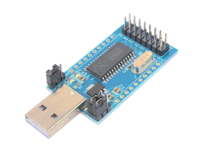
| CH341 | WCH (Jiangsu Qinheng) | UART/I2C/SPI | 3.3V / 5V | 2 Mbps |
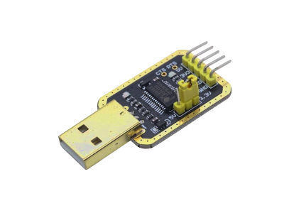
CH340
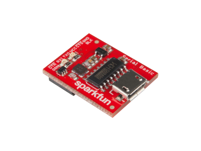
A common USB Serial Adapter is the CH340 IC. Sparkfun has a breakout board (DEV-14050) for this IC, shown in the figure below, which works with 5V and 3.3V systems and should auto install on most operating systems without the need for additional drivers.
This device uses the CH340G version of the IC with a USB Micro-B connector and operates at USB Full Speed that supports baud rates from 50bpsbits per second to 2MbpsMegabits per second.
There is a jumper on the rear of the board that controls the output voltage on the VCCVoltage Collector Collector (VCC) is the supply voltage at the collector of a transistor. The double subscript notation of repeating letters "CC" is used to denote a power supply voltage that is relative to ground. pin. By default, the board outputs 3.3V and has 3.3V signals. Changing this jumper to 5V will cause the board to output 5V on the VCCVoltage Collector Collector (VCC) is the supply voltage at the collector of a transistor. The double subscript notation of repeating letters "CC" is used to denote a power supply voltage that is relative to ground. pin with 5V signals.
There are two LEDLight Emitting Diodes on the board connected to TXTransmit (Green) and RXReceive (Yellow) as a way to see the serial traffic.
The pinout mimics the common DTR/RX/TX/VCC/CTS/GND pinout found on many FTDI-to-USB derivatives.
Power Pins
- VCC:
- Power supply 3.3V (default) or 5V
- GND:
- Common ground for power and logic.
Data Pins
- DTR:
- Data Terminal Ready. This pin is active low.
- CTR:
- Clear To Send control input. This pin is active low.
- RX:
- UARTUniversal Asynchronous Receiver-Transmitter data receive pin. This pin receives the serial input.
- TX:
- UARTUniversal Asynchronous Receiver-Transmitter data transmit pin. This pin sends the serial output.
CP2102
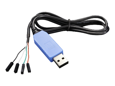
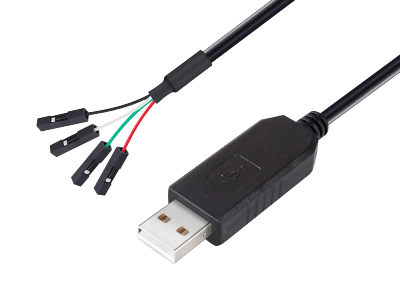
Another example of a common USB Serial Adapter is the Adafruit CP2102 shown in the figure below.
This device has a USB Type-A connector (USB Full Speed) with the SiLabs CP2102 chipset for 3.3V serial with a maximum transfer data rate of 921,600bpsbits per second.
This adapter has 4 leads with female Dupont connectors for power and data. The red lead is 5V @ 500mA direct from the USB port if you want to power an external device (if not then you can leave the red lead unattached). The black lead is ground. The white lead is the serial TXDTransmit Data and the green lead RXDReceive Data, both at at 3.3V.
CP2102N
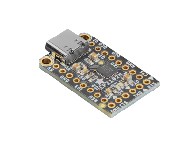
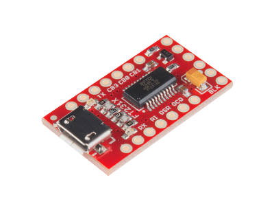
Another USB Serial Adapter is the Adafruit CP2102N shown in the figure below.
This device has a USB Type-C connector with the SiLabs CP2102N chipset compatible with either 3.3V and 5V serial. This adapter has a maximum transfer data rate of 3MbpsMegabits per second.
The pinouts on the CP2102N USB Adapter are:
Power Pins
- 5V pins:
- These are the 5V power pins. They receive 5V output from USB and can supply ~500mA peak.
- 3V pin:
- This is the 3.3V power pin. It is the output from the 3.3V regulator and can supply ~500mA peak
- GND pins:
- These are common ground for power and logic.
Data Pins
- CTS:
- Clear To Send control input. This pin is active low.
- TXD:
- UART data transmit pin. This pin sends the serial output.
- RXD:
- UART data receive pin. This pin receives the serial input.
- RTS:
- Ready To Send control output. This pin is active low.
FT232H
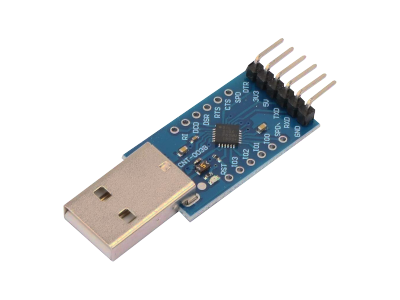
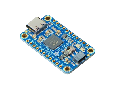
The Adafruit FT232H USB to GPIOGeneral Purpose Input Output Adapter shown in the figure below can read in multiple communication protocols: UARTUniversal Asynchronous Receiver-Transmitter, I2CInter-Integrated Circuit. Also referred to as IIC or I2C., and SPISerial Peripheral Interface.
This adapter has a few USB pins to read and write digital data to. However, you cannot use both the serial UART and Multi-Protocol Synchronous Serial Engine (MPSSEMulti-Protocol Synchronous Serial Engine) GPIO, SPI, I2C, etc. modes of the chip at the same time.
This device has a USB type-C connector with the FTDIFuture Technology Devices International FT232HQ chipset compatible with 3.3V serial and 5V tolerant. It has a maximum transfer data rate of 12Mbaud (UART) up to 40MB/s (Sync FIFOFirst In First Out). Most operating systems include FTDI's serial driver so manual installation of the driver is usually unnecessary.
The pinouts on the FT232H USB Adapter are:
Power Pins
- 5V:
- This is a 5 volt power source connected directly to the USB bus with a max current draw of 300mA.
- GND:
- This is the ground pin.
Data Pins
- D0 through D7:
- These are the ADBUS pins on the FT232H chip and are used for the serial UART and other serial protocols. You can also use some of them as GPIOGeneral Purpose Input Output pins for digital inputs and outputs.
- C0 through C9:
- These are the ACBUS pins on the FT232H chip and are mainly used as GPIOGeneral Purpose Input Output pins for digital inputs and outputs. Note that pins C8 and C9 are not controlled by software and can only be assigned functionality by changing the EEPROMElectrically Erasable Programmable Read-Only Memory of the chip.

(0) Comments
Sign in to leave a comment
Sign In