I2C Communication
Updated: 12Aug2024 02:01:10 UTC 2024-08-12T02:01:10Z
Rating: (0 reviewsThis article has not been rated yet)
Inter-Integrated Circuit (I2CInter-Integrated Circuit. Also referred to as IIC or I2C.) is a protocol intended to allow one or more controller devices to communicate with multiple peripheral devices. I2C operates on a synchronous bus that only uses two wires, a Serial Clock Line (SCLSerial Clock (SCL) is the output clock signal line from the master device. Also referred to as SCK, SCLK, or CLK.) and Serial Data Line (SDLSerial Data Line), for half-duplex communication over a short distance (it was originally designed to communicate between integrated circuits on the same PCBPrinted Circuit Board).
I2C uses a multi-master/multi-slave configuration that gives a microcontroller or SBCSingle Board Computer the capability of controlling a network of devices (e.g., sensors, LCDLiquid Crystal Displays, memory modules, etc.) with just two general purpose I/OInput/Output pins and software.
This introduction to I2C will cover its hardware wiring, data transmission, signals, speed, and software I2C.
Hardware Wiring
I2C is a synchronous bus that uses two wires, a Serial Line Clock (SCLSerial Clock (SCL) is the output clock signal line from the master device. Also referred to as SCK, SCLK, or CLK.) and Serial Data Line (SDLSerial Data Line), for half-duplex communication over a short distance. I2CInter-Integrated Circuit. Also referred to as IIC or I2C. is also referred to as a Two-Wire Interface (TWITwo-Wire Interface). It operates on the master-slave principle with the master as the main controller and peripheral devices as the slaves.
- SDL (Serial Data Line):
- used by the master or slave to transmit/receive data
- SCL (Serial Line Clock):
- used by the master to transmit the clock signal
Both the SDASerial Data Line and SCLSerial Clock (SCL) is the output clock signal line from the master device. Also referred to as SCK, SCLK, or CLK. lines have pull-up resistors (RPU) that are pulled up to VDDVoltage Drain Drain (VDD) is the supply voltage at the Drain of a transistor. The double subscript notation of repeating letters "DD" is used to denote a power supply voltage that is relative to ground. , the logic level supply of the master device (the supply voltage is not standard, so it can be 3.3V, 5.5V, or some other voltage). The I2CInter-Integrated Circuit. Also referred to as IIC or I2C. bus drivers are open drain drivers, which means they can drive drive their output low, but cannot drive it high. For the line to be able to go high there has to be pull-up resistors to VDDVoltage Drain Drain (VDD) is the supply voltage at the Drain of a transistor. The double subscript notation of repeating letters "DD" is used to denote a power supply voltage that is relative to ground. . Some devices already have pull-up resistors within them for the SDASerial Data Line and SCLSerial Clock (SCL) is the output clock signal line from the master device. Also referred to as SCK, SCLK, or CLK. pins, where external pull-up resistors are not needed.
One of the main advantages of I2CInter-Integrated Circuit. Also referred to as IIC or I2C. is the capability of adding as many peripheral devices as you want to the bus (SDASerial Data Line and SCLSerial Clock (SCL) is the output clock signal line from the master device. Also referred to as SCK, SCLK, or CLK. lines) as long as the maximum bus capacitance of 400pF is not exceeded. This is illustrated in the figure below.
Data Packets
I2C messages are sent on the SDA line in the form of a packet that consists of two types of frames: an address frame that contains the binary address of the slave that the master is sending the message to and one or more 8-bit data frames containing the contents of the message. The packet also includes start and stop conditions, read/write (R/W) bits, and ACKAcknowledgment/NACKNegative Acknowledgment bits between each data frame. It may also have a register address frame (after the device address frame) depending on the device.
Start Bit
The start condition indicates the beginning of a packet sent and puts all peripheral devices on notice that a transmission is about to start. This condition occurs when the master has leaves SCL HIGH and pulls the SDA LOW. That is, the SDA line switches from a high voltage level to a low voltage level before the SCL line switches from high to low.
Device Address Frame
The address frame is a 7 or 10 bit sequence unique to each slave that identifies the slave when the master wants to communicate with it. Most I2C devices use a 7-bit addressing scheme, but some newer devices use a 10-bit address. The address frame is always first in any new communication sequence. The 7-bit ordering of the address is MSBThe Most Significant Bit (MSB) in a binary number is the bit that represents the largest place value carrying the most weight. It is also sometimes referred to as the high-order bit or left-most bit due to the convention in positional notation of writing less significant digits further to the right. first and LSBThe Least Significant Bit (LSB) in a binary number is the bit that represents the smallest place value carrying the lowest weight. It is also sometimes referred to as the low-order bit or right-most bit due to the convention in positional notation of writing less significant digits further to the right. last, followed by a Read/Write (R/W) bit indicating whether this is a read (1) or write (0) operation, and then the NACK/ACK bit (this sequence is the same for both data and address frames).
Once the address and R/W of the frame are sent, the receiving device is given control over SDA. If the receiving device does not pull the SDA line low before the NACK/ACK bit clock pulse, it can be inferred that the receiving device either did not receive the data or did not know how to parse the message. If that is the case, the exchange stops, and it's up to the master device to decide how to proceed.
Register Address Frame
Some slave devices may require configuration upon startup to set the behavior of the device. This is typically done when the master accesses the slave's internal register maps and writes to a unique register addresses that is 8-bits with a bit ordering of MSB to LSB.
Read/Write (R/W) Bit
The R/W bit specifies whether the master is sending data to the slave (LOW voltage level) or requesting data from it (HIGH voltage level).
ACK/NACK Bit
Each frame in a message is followed by an acknowledge/no-acknowledge bit that determines if the frame was successfully received and another frame can be sent. If an address frame or data frame was successfully received, an ACKAcknowledgment bit is returned to the master from the slave device; otherwise a NACKNegative Acknowledgment bit is sent.
Before the slave can send an ACK, the master must release the SDA line. To send an ACK bit, the receiver pulls down the SDA line during the low phase of the ACK/NACK-related clock period, so that the SDA line is stable low during the high phase of the ACK/NACK-related clock period. Setup and hold times must be taken into account.
When the SDA line remains high during the ACK/NACK-related clock period, this is interpreted as a NACK. There are several conditions that lead to the generation of a NACK:
- The slave is unable to receive or transmit because it is performing some other function and is not ready to start communication with the master.
- During the transfer, the slave gets data or commands that it does not understand.
- During the transfer, the slave cannot receive any more data.
- A master-receiver is done reading data and indicates this to the slave through a NACK.
Data Frame
After the address frame has been sent, the data frame containg the contents of the message can begin being transmitted. The controller will simply continue generating clock pulses at a regular interval, and the data will be placed on SDA line by either the master or the slave, depending on whether the R/W bit indicated a read or write operation.
The data frame is 8-bits long and sent with a bit ordering MSB first and LSB last. Each data frame is immediately followed by an ACK/NACK bit to verify that the frame has been received successfully. The ACK bit must be received by either the master or the slave (depending on who is sending the data) before the next data frame can be sent. The number of data frames is arbitrary, and most peripheral devices will auto-increment the internal register, meaning that subsequent reads or writes will come from the next register in line.
Stop Condition
After all of the data frames have been sent, the master can send a stop condition to the slave to halt the transmission. The stop condition is a voltage transition from low to high on the SDA line after a low to high transition on the SCL line, with the SCL line remaining high. During normal data writing operation, the value on SDA should not change when SCL is high, to avoid false stop conditions.
Bit Ordering
The order in which the bits are transmitted over a communication channel is called Endianness. There are two types of endianness. Little-endian has the Least Significant Bit (LSBThe Least Significant Bit (LSB) in a binary number is the bit that represents the smallest place value carrying the lowest weight. It is also sometimes referred to as the low-order bit or right-most bit due to the convention in positional notation of writing less significant digits further to the right.) sent first and Most Significant Bit (MSBThe Most Significant Bit (MSB) in a binary number is the bit that represents the largest place value carrying the most weight. It is also sometimes referred to as the high-order bit or left-most bit due to the convention in positional notation of writing less significant digits further to the right.) sent last. Big-endian transmits the MSB first and the LSB last.
For example, suppose we want to send the number 45 serially over a transmission line. The number 45 is 00101101 in binary. Big-endian bit ordering would be transmitted left to right (00101101) and little-endian would be transmitted right to left (10110100). The endianness of a I2C transmission is big-endian.
I2C Signal
An I2C signal typically has voltage levels from 0V to +3.3V or 5V, although other voltage levels are permitted. When sending a transmission over I2C, both devices should have the same SDA and SCL signal voltage level (e.g., 3.3V to 3.3V or 5V to 5V). However, since the devices on the bus don't actually drive the signals high, I2C has some flexibility in connecting devices with different I/OInput/Output voltages.
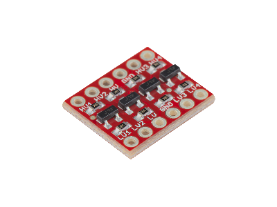
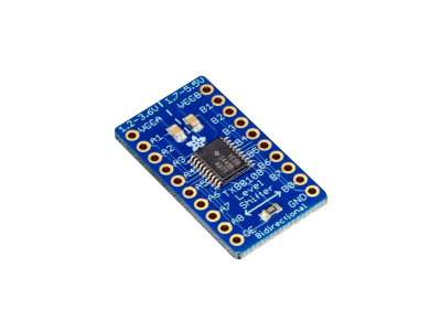
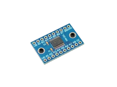
One way to hookup two devices at different voltages is to connect pull-up resistors to the lower of the two voltages, but this only works in some cases, where the lower of the two device voltages exceeds the high-level input voltage (i.e., enough to detect a HIGH level state in the signal). Otherwise, a BSS138 FETField Effect Transistor Logic Level Converter or a buffer/driver level shifter ICIntegrated Circuit is recommended (a list of options is provided in the Products section).
The HIGH/LOW voltage levels on the SDA (data) and SCL (clock) lines indicate when the transmission is idle, start/stop message delimiters, register address, data frame, and acknowledgment (ACK). An illustration of an I2C signal without a register address is shown in the figure below.
Before the transmission the I2C bus is idle and both the SDA (data) and SCL (clock) lines are held HIGH by the Master. The start of the transmission occurs when the SDA line switches from HIGH to Low before the SCL line switches from HIGH to Low.
Next is a sequence of logical bits for the address and data frames, R/W bit, and ACK/NACK bits, during which the SDA only transitions when SCL is low; otherwise it would be interpreted as a start and stop condition. The stop condition occurs when the voltage transitions from LOW to HIGH on the SDA line after a LOW to HIGH transition on the SCL line. The SDA and SCL lines both remain high in idle until the next transmission.
Transmission Speed
The original I2C bus had a maximum speed of 100kHz, now called the standard mode. Most applications still use this speed, since it is usually sufficient for transferring data with most modules, such as sensors, memory modules, and LCDLiquid Crystal Display displays. The I2C protocol specifies this standard mode and higher speed modes, as given in the table below, but not all I2C devices support these modes.
| Mode | Speed |
|---|---|
| Standard Mode (Sm) | 100kbps |
| Fast Mode (Fm) | 400kbps |
| Fast Mode Plus (Fm+) | 1Mbsp |
| High-Speed Mode (Hs) | 3.4Mbps |
| Ultra-Fast Mode (UFm) | 5Mbps |
Software I2C
If a device such as a microcontroller or SBCSingle Board Computer doesn't have a I2C port or enough of them for your application, then the digital I/OInput/Output pins can be controlled by the processor to emulate I2C (a technique known as Bit Banging). There are libraries available, like the Arduino SoftWire, SoftI2CMaster, and Arduino_SoftWareI2C that make this more convenient for serial interfaces. Bit-banging is more processor-intensive, not as reliable, and not as fast as a hardware I2C port, but it can be useful when needed.
Conclusion
This introduction to I2C covered its hardware wiring, data packet structure, bit ordering, signals, transmission speed, and software I2C. There are advantages and disadvantages to using I2C compared to other wired communication protocols such as UARTUniversal Asynchronous Receiver-Transmitter and SPISerial Peripheral Interface.
Some of the advantages of using I2C are:
- It only requires only two data lines for transmission.
- Allows one or more controller devices to communicate with multiple peripheral devices.
- The ACK/NACK bit confirms each frame has been transferred successfully.
Some of the disadvantages of using I2C are:
- The size of the data frame is very limited to only 8-bits.
- You need a library or write your own software to specify the unique register addresses of devices.
- There are no message error checking bits.
- The speed is lower than SPI.
However, I2C is well known with plenty of documentation and is widely used for bidirectional communication between devices.





(0) Comments
Sign in to leave a comment
Sign In