Analog-to-Digital Converter (ADC) ICs and Modules
Updated: 26Aug2024 20:20:56 UTC 2024-08-26T20:20:56Z
Rating: (0 reviewsThis article has not been rated yet)
Analog signals are converted to digital data using an Analog-to-Digital Converter (ADCAnalog-to-Digital Converter (ADC, A/D, or A-to-D)). The goal of the ADC is to accurately represent analog signals as digital data, a process that involves sampling, quantization, and encoding.
Most microcontrollers include an internal ADC with interface pins to read analog inputs, but the resolution and number of channels are limited. Most Single Board Computers (SBCSingle Board Computers) do not have an internal ADC, so an external ADC is needed to read analog inputs.
There are many external ADCs packaged in ICIntegrated Circuits and modules with I2CInter-Integrated Circuit. Also referred to as IIC or I2C. or SPISerial Peripheral Interface communication interfaces. This overview covers ADC specs and the different kinds of ADC ICs and Modules.
ADC Specs
Sampling Rate
The sampling rate quantizes the analog signal in the time domain. How fast of an ADC sampling rate is needed depends on your application. Some applications require high sampling rates while others can use a low sampling rate.
For example, high sampling rates are needed with the conversion of an audio signal: the human voice signal contains frequency components that span from 20Hz to 4kHz. Low sampling rates are needed, for example, measuring the temperature of your house or monitoring a battery level, where it is acceptable to take samples at intervals of several seconds, minutes, hours, or even days.
From the Nyquist Theorem, the minimum sampling rate must be at least double the highest frequency content of the signal in order to render a faithful reconstruction of the original signal. In practice, as a rule of thumb, a minimum sampling rate of at least 5x to 10x the highest frequency content is chosen to give a decent representation of the original signal.
Some ADCs have two different conversion modes: single-shot and continuous. In single-shot mode, the ADC performs one conversion of the input signal upon request and stores the value in an internal data buffer. The device can then enter a low-power state to save power until the next request is made. In continuous conversion mode, the ADC automatically begins a conversion of the input signal as soon as the previous conversion is completed.
Resolution
An analog signal is quantized in amplitude by its discrete digital representation. The resolution of an ADC indicates the number of different discrete values it can produce over the allowed range of analog input values. This defines the smallest step size change that can be measured by the ADC, often referred to as quantization error.
Resolution can be expressed as the bit depth n where the number of discrete values available is 2n. For example, an ADC with a resolution of 10-bits can encode an analog input to one of 210 different levels from 0 to 1023. According to this definition of resolution, a higher value with more levels has better resolution.
Resolution can also be defined electrically expressed in volts. The change in voltage required to guarantee a change in the output level is called the Least Significant Bit (LSBThe Least Significant Bit (LSB) in a binary number is the bit that represents the smallest place value carrying the lowest weight. It is also sometimes referred to as the low-order bit or right-most bit due to the convention in positional notation of writing less significant digits further to the right.) voltage. The resolution of an ADC is equal to the LSBThe Least Significant Bit (LSB) in a binary number is the bit that represents the smallest place value carrying the lowest weight. It is also sometimes referred to as the low-order bit or right-most bit due to the convention in positional notation of writing less significant digits further to the right. voltage as given in the figure below. According to this definition of resolution, a lower value has better resolution.
Channels
An ADC IC or module typically has one ADC that can read from 2, 4, 6, or 8 channels through a multiplexer (MUXA Multiplexer (MUX) is a device that selects between several analog or digital input signals and forwards the selected input to a single output line.), a kind of switch that operates on any one of these inputs at a time.
Some channels may be used to read its voltage reference, the ground potential, an internal temperature sensor, or differential inputs (where the quantity measured is the difference between two inputs). When programming a microcontroller or SBC to read an ADC, you must tell it which channel to convert from and only one channel can be used in the conversion at a time.
ADC ICs
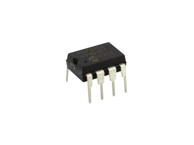
MCP3002 10-Bit ADC
The MCP3002 10-Bit ADC IC shown in the figure below is a common IC used for converting analog signals from sensors to the digital SPISerial Peripheral Interface communication protocol.
The MCP3002 has the following features:
- 2 channels of 10-bit analog input.
- 3 pins are required for the SPI digital output.
- Supply voltage from 2.7V to 5.5V with low power consumption (5nA typical standby, 375µA typical active).
- The maximum sampling rate is 200ksps when supplied with 5V and 75ksps when supplied with 2.7V.
More details on the MCP3002 IC can be found in the MCP3002 Datasheet (PDF).
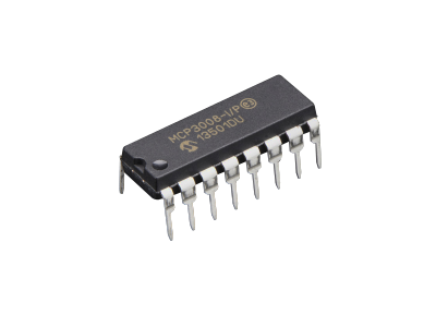
MCP3008 10-Bit ADC
The MCP3008 10-Bit ADC IC shown in the figure below is a popular choice for converting analog signals from sensors to the digital SPI communication protocol.
The MCP3008 has the following features:
- 8 channels of 10-bit analog input.
- 4 pins are required for the SPI digital output.
- Supply voltage from 2.7V to 5.5V with low power consumption (5nA typical standby, 425µA typical active).
- The maximum sampling rate is 200ksps when supplied with 5V and 75ksps when supplied with 2.7V.
More details on the MCP3008 IC can be found in the MCP3008 Datasheet (PDF).
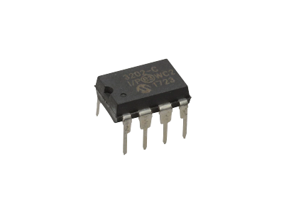
MCP3202 12-Bit ADC
The MCP3202 12-Bit ADC IC shown in the figure below is another well known chip used for converting analog signals from sensors to the digital SPI communication protocol.
The MCP3202 has the following features:
- 2 channels of 12-bit analog input.
- 3 pins are required for the SPI digital output.
- Supply voltage from 2.7V to 5.5V with low power consumption (500nA typical standby, 550µA typical active).
- The maximum sampling rate is 100ksps when supplied with 5V and 50ksps when supplied with 2.7V.
More details on the MCP3202 IC can be found in the MCP3202 Datasheet (PDF).
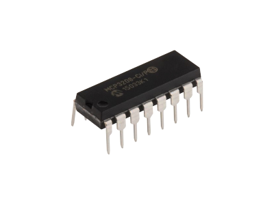
MCP3208 12-Bit ADC
The MCP3208 12-Bit ADC IC shown in the figure below is similar to the MCP3202, but has a larger package size with 8-channels instead of only 2-channels.
The MCP3208 has the following features:
- 8 channels of 12-bit analog input.
- 3 pins are required for the SPI digital output.
- Supply voltage from 2.7V to 5.5V with low power consumption (500nA typical standby, 400µA typical active).
- The maximum sampling rate is 100ksps when supplied with 5V and 50ksps when supplied with 2.7V.
More details on the MCP3208 IC can be found in the MCP3208 Datasheet (PDF).
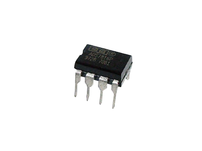
ADS7816 12-Bit ADC
The ADS7816 12-Bit ADC IC shown in the figure below can be used for converting a single channel or differential input analog signal with a digital 3-wire SPI communication interface.
The ADS7816 has the following features:
- Single channel or differential input.
- 3-wire SPI communication interface.
- Supply voltage from 4.5V to 5.25V with low power consumption (30μA at 12.5ksps and 380μA at 200ksps).
- Maximum sampling rate of 200kHz.
More details on the ADS7816 IC can be found in the ADS7816 Datasheet (PDF).
ADC Modules
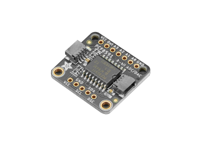
PCF8591 8-Bit ADC
The PCF8591 8-Bit ADC/DACDigital-to-Analog Converter (DAC, D/A, or D-to-A) module by Adafruit (PID 4648) shown in the figure below has a low resolution ADC for converting analog signals from sensors to the digital I2CInter-Integrated Circuit. Also referred to as IIC or I2C. communication protocol.
The PCF8591 has the following features:
- 4 channels of 8-bit analog input.
- 2 pins (SCLSerial Clock (SCL) is the output clock signal line from the master device. Also referred to as SCK, SCLK, or CLK., SDASerial Data Line) are required for the I2C digital output.
- One pin (Out) for an 8-bit DAC output.
- Supply voltage from 2.5V to 6.0V.
- The maximum sampling rate is 11.1ksps.
Adafruit has a guide on their PCF8591 board, including an Arduino Library, CircuitPython Library, schematics, and PCB. More details can be found in the in the following links.
ADS1015 12-Bit ADC
The Texas Instruments ADS1015 IC is a low power 12-Bit ADC with an I2C interface that has a programmable sample rate from 128spsSamples Per Second to 3300spsSamples Per Second.
The ADS1015 has the following features:
- 4 single-ended input channels or two differential channels.
- Programmable gain amplifier up to x16 to help boost up smaller single/differential signals to the full range.
- 2V to 5.5V power/logic and low power consumption with only 150µA in continuous mode and a single-shot mode that automatically powers down after conversion.
More details about this IC can be found on the TITexas Instruments product page TI ADS1015 Product Page and in the ADS1015 Datasheet (PDF).
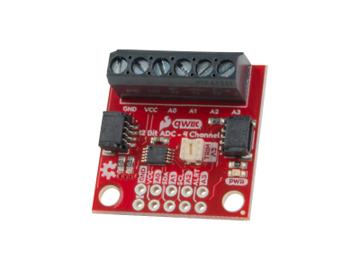
The SparkFun ADS1015 12-bit ADC module (DEV-15334) can provide four channels of I2C controlled ADC input through QwiicQwiic connectors are SparkFun's name for 4-pin JST SH connectors with 1.0mm pitch. These connectors were implemented on SparkFun boards to make it easy to plug-n-play various sensors and devices without soldering and wiring. Qwiic is cross-compatible with Adafruit's STEMMA QT connectors. connectors or 0.1in spaced pins in case you prefer to use a breadboard.
This ADC board includes screw pin terminals on the four channels of input, allowing for solderless connection to voltage sources in your setup. It also has an address jumper that lets you choose one of four unique addresses (0x48, 0x49, 0x4A, 0x4B), so you can connect up to four of these on the same I2C bus and have sixteen channels of ADC.
There is an onboard 10kΩ trimpot connected to channel A3. This is handy for initial setup testing and can be used as a simple variable input to your project (an isolation jumper is included so you can use channel A3 however you like).
SparkFun has a hookup guide on their ADS1015 board, an Arduino Library, and schematics. More details can be found in the in the following links.
- SparkFun ADS1015 Product Page
- GitHub SparkFun ADS1015 Product Repo
- SparkFun ADS1015 Hookup Guide
- GitHub SparkFun ADS1015 Arduino Library
- SparkFun ADS1015 Board Schematic (PDF)
The Adafruit ADS1015 12-Bit ADC breakout module board (PID 1083) has 0.1" pin separation and comes with a standard header in case you want to use it with a breadboard or perfboard.
Four mounting holes are on each corner of the board for easy attachment and both ends of the board have a JST SH 1.0mm pitch connector allowing solderless connections between the board and external devices.
Adafruit has a guide on their ADS1015 board, an Arduino Library, CircuitPython Library, and schematics. More details can be found in the in the following links.
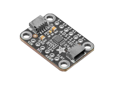
ADS1115 16-Bit ADC
The Texas Instruments ADS1115 IC is a small low power 16-Bit ADC with an I2CInter-Integrated Circuit. Also referred to as IIC or I2C. interface.
The ADS1115 IC has the following features:
- Can be configured as 4 single-ended input channels or two differential channels.
- Programmable sample rate from 8SPSSamples Per Second to 860SPSSamples Per Second.
- Programmable gain amplifier up to x16 to help boost up smaller single/differential signals to the full range.
- Supply voltage from 2V to 5V power/logic and low power consumption with only 150µA in continuous mode and a single-shot mode that automatically powers down after conversion.
More details about the ADS1115 IC can be found on the TI ADS1115 Product Page and in the ADS1115 Datasheet (PDF).
The Adafruit ADS1115 16-Bit ADC breakout board has STEMMA QTSTEMMA QT ('cutie') connectors are Adafruit's name for 4-pin JST SH connectors with 1.0mm pitch. These connectors were implemented on Adafruit boards to make it easy to plug-n-play various sensors and devices without soldering and wiring. The STEMMA QT (JST SH) are a smaller connector than the STEMMA (JST PH) that do not fit on smaller boards. STEMMA QT is cross-compatible with SparkFun Qwiic connectors. connectors for power and I2C, allowing solderless connections between the board and external devices. The board also has pin through holes with 0.1" pin separation in case you want to use it with a breadboard or perfboard (the board comes with a separate 16-pin male header).
Adafruit has a guide on their ADS1115 board, an Arduino Library, CircuitPython Library, and schematics, which are the same for their ADS1015 board. More details can be found in the in the following links.
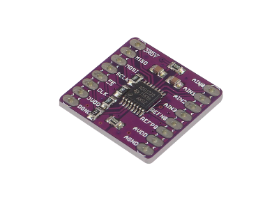
ADS1220 24-Bit ADC
The ADS1220 is a high precision 24-bit ADC with an SPI interface that can be used for applications measuring small sensor signals, such as resistance temperature detectors (RTDs), thermocouples, thermistors, and resistive bridge sensors (Pressure Sensors, Strain Gauges, and Weigh Scales).
The ADS1220 has the following features:
- 4 channels that can act as two differential input channels.
- Low noise Programmable Gain Amplifier (PGAA Programmable Gain Amplifier (PGA) is an electronic amplifier whose gain can be controlled by external digital or analog signals.) from 1 V/V to 128 V/V.
- Programmable data rates up to 2ksps.
- Supply voltage from 2.3V to 5.5V.
The ADS1220 has two available conversion modes: single-shot and continuous. In single-shot mode, the ADC performs one conversion of the input signal upon request and stores the value in an internal data buffer. The device then enters a low-power state to save power. In continuous conversion mode, the ADC automatically begins a conversion of the input signal as soon as the previous conversion is completed.
More details on the ADS1220 IC can be found in the in the ADS1220 Datasheet (PDF).
ADC Comparison
The table below provides a spec comparison of the ADCs covered in this article, organized by increasing resolution. When selecting an ADC, there is a trade-off between resolution and sampling rate. A higher resolution ADC usually has a lower sampling rate because the ADC needs to process more bits per conversion cycle.
| ADC IC | Resolution | Channels | Sample Rate | COMCommunication | Datasheet |
|---|---|---|---|---|---|
| PCF8591 | 8-Bit | 4-Channel | Up to 11.1ksps | I2C | PCF8591 Datasheet (PDF) |
| MCP3002 | 10-Bit | 2-Channel | 75ksps - 200ksps | SPI | MCP3002 Datasheet (PDF) |
| MCP3008 | 10-Bit | 8-Channel | 75ksps - 200ksps | SPI | MCP3008 Datasheet (PDF) |
| MCP3202 | 12-Bit | 2-Channel | 50ksps - 100ksps | SPI | MCP3202 Datasheet (PDF) |
| MCP3208 | 12-Bit | 8-Channel | 50ksps - 100ksps | SPI | MCP3208 Datasheet (PDF) |
| ADS7816 | 12-Bit | 1-Channel | Up to 200ksps | SPI | ADS7816 Datasheet (PDF) |
| ADS1015 | 12-Bit | 4-Channel | 128sps - 3300sps | I2C | ADS1015 Datasheet (PDF) |
| ADS1115 | 16-Bit | 4-Channel | 8sps - 860sps | I2C | ADS1115 Datasheet (PDF) |
| ADS1220 | 24-Bit | 4-Channel | 5sps - 2ksps | SPI | ADS1220 Datasheet (PDF) |


(0) Comments
Sign in to leave a comment
Sign In