Interfacing Analog Inputs
Updated: 07Aug2024 00:28:40 UTC 2024-08-07T00:28:40Z
Rating: (0 reviewsThis article has not been rated yet)
This article shows how to interface analog signals so they are compatible with an ADCAnalog-to-Digital Converter (ADC, A/D, or A-to-D). This is known as Signal Conditioning, the modification of a signal to prepare it for the next stage of processing. The type of signal conditioning covered here involves scaling and/or offsetting a signal to the input range of the ADC.
If an analog signal exceeds the range of the ADC, attenuation of the signal can be implemented with a simple voltage resistor divider. This works for low frequency signals (usually < 50Hz) with a low sampling rate. For higher frequency signals, where higher sampling rates are required, the impedance of the resistor divider may not provide enough current and time needed by the sampling capacitor in an ADC to charge up sufficiently to accurately sample the signal. This problem can be resolved by using a unity gain OpAmpOperational Amplifier voltage follower as a buffer to provide low impedance into the ADC.
An ADC is limited to only capturing positive voltages. If the input signal is expected drop below zero, like it does in ACAlternating Current signals, an offset in voltage called a DCDirect Current bias can be injected into the signal to shift it to the positive range for the ADC.
Since the range of input signals can be larger or smaller than the ADC range, a more flexible analog front end design would have the capability of adjusting the amount of signal attenuation or amplification to cover as much as the ADC range as possible in order to maximize the signal resolution. A design using a differential amplifier Operational Amplifier (OpAmp) with potentiometers to tune the signal gain and offset will be discussed.
Resistor Voltage Divider
A resistor voltage divider is a simple circuit that converts a large voltage into a smaller voltage. It consist of two or more resistors in series that divide an input voltage source across each resistor by an amount that depends on the resistance. This section will explain how resistor dividers work, their use in voltage sensor modules, and their limitations.
Resistor Voltage Divider Circuit
The resistor voltage divider circuit shown in the figure below consist of two resistors in series that divide an input source voltage VS across the resistors R1 and R2.
The voltages across both of the resistors given below is determined from Ohm's Law and Kirchhoff's Voltage Law. The attenuated output voltage (V2) is usually taken across the second resistor (R2) and is directly proportional to the input voltage (VS) and the ratio of the R2 resistor to the sum of R1 and R2 resistors. The ratio of the resistances can range from 0 to 1 as a scalar of the input voltage (VS), which means the output voltage can from be anywhere from 0V to VS depending on the resistor values chosen.
The choice of resistor values depend on the how much voltage needs to be attenuated along with trade-offs between minimizing power consumption, generating sufficient output current, limiting the impedance into an ADC, and staying under maximum power ratings the resistors can handle. Having small resistors gives more output current with less source impedance for an ADC, but consumes more power which would be a concern for battery applications and possibly exceeding the power limits of the resistors. Having large resistance reduces the current with less power consumption, but must be under the maximum source impedance of the ADC (usually around 5kΩ - 10kΩ), and the signal is more influenced by noise (parasitic capacitance has a much more noticeable effect). Online calculators that search for standard resistor values are available, like the one at howardtechnical.com.
For measuring voltages accurately, you also want to make sure the error tolerances of the resistors are low with precision resistors (1% tolerance or less). The International Electrotechnical Commission (IECInternational Electrotechnical Commission) defines resistance and tolerance values in the following E-Series:
- E12:
- 10% tolerance
- E24:
- 5% tolerance (also available with 1%)
- E48:
- 2% tolerance
- E96:
- 1% tolerance
- E192:
- 0.5%, 0.25%, 0.1% and higher tolerances
The most common resistors provided below are the E24 and E96 series with 5% and 1% tolerances.
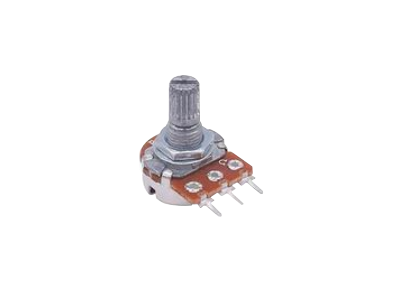
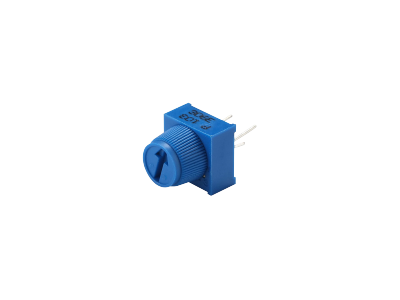
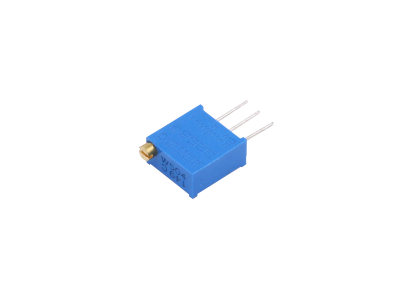
The potentiometers given below can also be used as a resistor divider and typically have a tolerance of 5%.
Voltage Sensor Module
The voltage sensor module illustrated below is a convenient device to measure voltages beyond the range of your ADC. It is small (typically 4cm x 3cm x 2cm dimensions), portable, and easy to hook up. This sensor incorporates a resistor voltage divider that makes the input voltage 5 times smaller. When used with a 5V range ADC, such as an Arduino Uno R3 or Nano, this sensor has an input voltage range of up to 25V. When used with a 3.3V range ADC, such as a RPiRaspberry Pi Pico or ESP32, this sensor has an input voltage range of about 16V.
The inputs and outputs of this sensor module are provided in the table below.
| Pin | Function |
|---|---|
| VCC | Input positive terminal of the external voltage source being measured. |
| GND | Negative terminal of the external voltage source (ground) |
| S | Analog output pin voltage to connect to your ADC |
| + | Not connected |
| - | Ground connection pin to the device that reads in the analog voltage. |
A schematic of the voltage sensor is given below.
Resistor Voltage Divider Limitations
There are a few limitations with resistor voltage dividers.
- Output has high impedance that can be a problem for an ADC.
- Only attenuates signals and cannot amplify a signal. Small signals relative to your ADC range need to be amplified to maximize the resolution.
- No over-voltage protection.
- Inefficient with power from dissipation by Joule's heating. For high-power applications, reactive voltage dividers using capacitors and/or inductors are preferred because they do not dissipate as much power as resistors.
Impedance Buffering
A resistor voltage divider adds source impedance when connected directly to an ADC. This impedance slows down the charging process of the ADC sample and hold capacitor CS/H within the sampling time. The ADCs in a microcontroller typically require the source impedance to be under 5kΩ - 10kΩ. If the impedance is too high, the sample and hold capacitor will not charge sufficiently to capture the variation in higher frequency signals (> 50Hz) where a high sampling rate is needed, resulting in inaccurate (attenuated) signal samples.
A unity-gain Operational Amplifier (OpAmp) known as a voltage follower can act as a buffer that prevents the sensor and voltage divider circuit from exceeding the maximum input impedance of the ADC (the OpAmp ideally has zero output impedance and practically < 100Ω).
OpAmp Voltage Follower
An OpAmp Voltage Follower configuration is given in the figure below. VS+ and VS- refers to the voltages applied to the OpAmp for its power supply (often called the rails). Some OpAmps use dual power supply ±VS and some use a single power supply +VS.
The negative feedback into the (-) terminal will attempt to make V+ - V- = 0. Since Vout = V+ = V-, this configuration gives a gain of 1. This means the OpAmp has no amplification nor attenuation of the input signal (Vin) and its main purpose is to provide a very low output impedance for an ADC.
The output voltage range of an OpAmp is contained within the voltages of the power supply rails (VS+ and VS-): you cannot get more than the supply puts in. Most OpAmps can't quite reach the supply range and their actual range is slightly within the rails (how much within the rails depends on the OpAmp and the load). An Opamp is saturated when the output cannot become any greater (or less) as illustrated in the figure below.
OpAmp saturation can provide some over-voltage protection to an ADC when the supply rails are set to the limits of the ADC range, provided that the input voltage level does not exceed the OpAmp's input voltage range specification. OpAmps typically have internal ESDElectrostatic Discharge protection diodes that are forward biased and start conducting current when the input spec range is exceeded for a very short time period (a fraction of a second). However, out of spec input voltages for a longer duration, called electrical overstress (EOS), can fry these internal protection diodes and damage the OpAmp.
Resistor Voltage Divider with OpAmp Buffer
Adding unity-gain OpAmp voltage follower as a buffer between a resistor voltage divider and ADC, as shown in the figure below, allows higher R2 resistor values (> 5kΩ - 10kΩ) to be used that can lower power consumption and measure higher frequency signals.
Since the OpAmp has unity-gain, the output voltage is simply the voltage from the resistor divider across R2.
Negative Voltages and DC Bias
An ADC is limited to only capturing positive voltages, but what if we wanted to read in voltages that drop below zero like AC signals? One way to do this is to shift the negative voltages by a constant amount to make them positive voltages, then read in the positive signal with an ADC, and finally in software shift the data back to the original signal with negative values. Shifting signals by a constant amount in hardware is known as injecting a DC bias into the signal, as shown in the figure below with +VBias.
The output voltage that results from this circuit is simply the sum of the voltages from the resistor divider and the bias voltage given below.
It is often the case where you do not have the exact bias voltage available from a source. You could use a resistor voltage divider to scale down a larger reference voltage (VRef) to the bias value you need (either using fixed resistors or an adjustable potentiometer). The reference voltage could come from the power supply of a microcontroller (3.3V or 5V) or some other external source. This is shown in the schematic below.
The output voltage that results from from a divided reference voltage is given below.
An example of converting a ±12V AC sinusoidal signal down to the 0V to 5V range of an ADC is shown below. This signal is first attenuated 5x smaller (from ±12V to ±2.4V) by a voltage divider with the same resistors commonly found in a voltage sensor module. The signal is then DC biased by VBias = +2.5V going into the positive terminal of a unity-gain OpAmp buffer (±2.4V + 2.5V gives a range of 0.1V to 4.9V). The output of the OpAmp (0.1V to 4.9V) is the signal that would be fed into an ADC.
Gain and Offset
The circuits in the previous sections are good for attenuating signals that are larger than the ADC range, but what about amplifying signals? A signal that covers more the ADC range will have the best resolution of the sampled signal (i.e., finer steps in the voltage can be observed). An ADC has discrete step sizes with a resolution determined by the voltage range and number of bits of the ADC (e.g., 8-bit ADC, 10-bit ADC, 12-bit ADC, etc.). For example, a 10-bit ADC with a 5V range gives a resolution of 1mV. Small signals that vary over a few millivolts will be heavily discretized due to the limited resolution of an ADC. To overcome this, the signal needs to be amplified with a gain on the signal.
Having control over the signal gain, where you can adjust the amount of signal amplification or attenuation, to make the signal cover as much as the ADC range as you want would be a more flexible analog front end design. There are many ways to accomplish this, but one of the simplest ways is using a differential amplifier OpAmp configuration where the signal gain and offset can be adjusted with with potentiometers.
Differential Amplifier
The differential amplifier shown in the figure below takes the difference of the voltages between the inputs with each input voltage is scaled by the resistors.
The output voltage from the differential amplifier in terms of the input voltages and resistors is given below. You can see that if all the resistors are equal and non zero, then the output voltage reduces to the difference of the input voltages V1 - V2.
Inverting Gain and Offset
The gain of the differential offset can be set by the resistance ratio R4/R2 and the offset by first term. Let V2 be in the input voltage and V1 be the reference voltage used for the offset.
This is an inverting circuit because the output signal will be inverted relative to the input signal. The gain and offset parameters can be made adjustable by replacing the resistors with potentiometers, as shown in the figure below. Once the gain is adjusted, the offset can be set. Since the amount of offset depends on the gain, the offset will have to be readjusted if the gain setting changes. Also note that the sensitivity of tuning the offset will increase with higher gain settings.
An example of using the differential amplifier to gain and offset a signal from ±5V to 0V - 3.3V is given in the figure below. First the potentiometer on the gain is adjusted to bring the ±5V signal down to ±3.3V. Next the potentiometer on the offset is adjusted to shift the signal by +3.3V. The resulting output signal is now 0V - 3.3V range, but inverted. This signal inversion can be fixed in software in a microcontroller or computer by subtracting the signal from the maximum ADC value.
Selecting OpAmps
When selecting an OpAmp for an analog front-end it is essential to know the characteristics of the OpAmp as specified in their datasheets. The following are OpAmp terms and parameters you commonly find specified in datasheets.
Terms and Parameters
- OpAmp Technology:
- OpAmps are made with different transistor technologies (Bipolar/BJTBipolar Junction Transistor, JFETJunction Field Effect Transistor, or MOSFETMetal-Oxide-Semiconductor Field-Effect Transistor/CMOSComplementary Metal-Oxide Semiconductor). Each has its own benefits and limitations. Bipolar OpAmps may have higher gain, lower input offset voltage, faster response, and higher operating voltages, whereas FETField Effect Transistor and CMOS OpAmps can provide rail-to-rail operation with very low input bias currents, high input resistance, and less power consumption. Some OpAmps combine technologies (bipolar and JFET as BiFET, bipolar and CMOS as BiCMOS) in the same device to get the best of both worlds.
- Supply Voltages:
- Refers to the voltages applied to the OpAmp for its power supply. Some OpAmps use dual power supply ±VS and some use a single power supply +VS. The supply voltage can be specified as a range VS = (V+) - (V-), indicating the total voltage between the two supply terminals. For example, the LM358 supply voltage range is 3V to 30V. This could be ±15V (a range of 30V), or at the lower extreme ±3V (a range of 3V), as long as the range is not smaller than 3V or larger than 30V.
- Input Voltage Range:
-
The range of voltages that an OpAmp can accept on its input pins. This parameter has two components that should
be considered: near-ground sensing and near rail sensing. The OpAmp may not be
able to sense voltages close to ground (e.g., < 10mV), even though the OpAmp may be able to go
down to or even cross 0V. If your OpAmp is being used to sense very small voltages, then
near-ground sensing should be a requirement when selecting an OpAmp. Input
voltages near the OpAmp power supply rails may also not be detectable if the input range doesn't extend out
close enough to the rails. If sensing near the rails is desired, then Rail-to-Rail
inputs should be a requirement when selecting an OpAmp.
When both input terminals have the same voltage, called a common-mode configuration, the input voltage is the common-mode voltage (VCM). If this common mode voltage gets too high or too low, the inputs will shut down and proper operation of the OpAmp ceases. The common mode input voltage range (VCMR or VICR) specifies the range over which normal operation is guaranteed. The common-mode voltage range is usually specified relative to the positive and negative supply voltage rails, where it could be within the rails, at the rails, or extend beyond the rails. It is typically dependent on the supply voltage (VS). For example, the LM358 common mode voltage range is (V-) to (V+) - 1.5 when VS is 3V to 36V. The MCP6002 has a common mode voltage range of VSS - 0.3V to VDD + 0.3V where VSS = GND and VDD = +1.8V to +5.5V.
The maximum differential mode input voltage is defined as the maximum allowable input voltage difference between the two input terminals of the OpAmp. When the input voltage difference of the OpAmp exceeds this voltage, the input stage of the OpAmp may be damaged. The specification is typically provided as an absolute minimum and maximum rating. For example, the LM358 differential voltage absolute minimum at -32V and an absolute maximum at 32V. - Output Voltage Swing:
-
Refers to how close the output voltage can reach the supply voltages (i.e., how much the output can be
driven rail-to-rail). This is often denoted by VOH and VOL,
but could be simply denoted as VO. The output voltage swing depends on the load and output current.
The output voltage swing for the LM358 is about 1.5V from the positive rail and 1V from the negative rail, with some small variation depending on the output current. These large voltages from the rails becomes an issue for low voltage (5V or 3.3V) devices such as microcontrollers and SBCs. For example, imagine trying to level shift a 0V - 5V sensor output range down to a 0V - 3.3V ADC range on a 3.3V microcontroller using an LM358. Setting the OpAmp positive supply to 3.3V and the negative supply to 0V, the maximum output is going to be clipped at about 3.3V - 1.5V = 1.8V and the minimum output will be clipped at about 0V + 1V = 1V. Having a 1V to 1.8V output range makes the LM358 a bad choice for this kind of application. A rail-to-rail OpAmp, like the MCP6002 or TLV2462, that can be driven on the order of millivolts from the rails, is more appropriate. - Open Loop Voltage Gain (Avol):
- This is the gain (Vout/Vin) of the OpAmp when there is no feedback implemented. The open loop gain is exceedingly large (10,000+), so it is usually specified in dBDecibel (dB) used to express the ratio of two physical quantities such as power, sound intensity, sound pressure, voltage, and current on a logarithmic scale. [20log10(Vout/Vin)] or the voltage ratio [V/mV]. High open-loop gains have more stable output in closed-loop configurations for temperature and signal variations.
- Common Mode Rejection Ratio (CMRRCommon-Mode Rejection Ratio):
- Defined as the ratio of the differential voltage gain to the common-mode voltage gain (ADIF/ACOM), usually expressed in dBDecibel (dB) used to express the ratio of two physical quantities such as power, sound intensity, sound pressure, voltage, and current on a logarithmic scale. [20log10(ADIF/ACOM)] or a voltage ratio [μV/V]. This refers to the error in balancing the inputs that quantifies the ability of the OpAmp to reject common-mode signals on both inputs. A higher CMRR value means better performance of the OpAmp. A high CMRR is required when a differential signal must be amplified in the presence of large common-mode input, such as noise.
- Input Impedance:
- The impedance between the non-inverting and inverting inputs of the OpAmp. Generally OpAmps have a high input impedance (in mega ohms or higher). Sometimes you see both the resistive (Ω) and capacitive (pF) components of the impedance specified. There are also two different modes the input impedance is specified for: common-mode and differential mode.
- Output Impedance:
- The resistance (denoted RO or ZO) between the output terminal of the OpAmp and the ground or common reference. The output impedance means the ratio of the voltage change to the corresponding current change. OpAmps usually have a very low output impedance. The output resistance of an OpAmp also depends on its external circuitry and if negative feedback is being used (negative feedback often lowers the output resistance).
- Input Offset Voltage:
- If the same voltage is applied to the input terminals, then ideally the output voltage should be zero. However, because the transistors inside the OpAmp do not have the same value, a small voltage appears on the output. The offset voltage (VOS) is the differential voltage between the two input terminals of an OpAmp that must be applied to null the output. This offset voltage should be close to zero, typically a few millivolts.
- Input Offset Current:
- If both the inputs to an OpAmp are grounded, then ideally the output current should be zero. However, because the base current to the transistors inside the OpAmp do not have the same value, a small current appears on the output. The offset current (IOS) is difference of the currents IB = |(IB+ - IB-)| flowing into the input terminals of an OpAmp to null the output current. This offset current should be close to zero, typically in nA or even pA.
- Input Bias Current:
- The average of the currents flowing into the input terminals of an OpAmp: IB = (IB+ + IB-)/2. The magnitude of this leakage current is small: on the order of picoamps (pA). Usually the smaller the input bias current, the smaller the output drifts.
- Gain Bandwidth GBW:
- The maximum frequency of the input when the voltage gain is 1 in an open loop configuration. Generally for low power applications GBW < 1MHz, for general purpose applications GBW is 1MHz to 10MHz, and for high speed applications GBW >10MHz. There are two main bandwidth parameters that characterize the frequency response of OpAmps: Unity Gain Bandwidth (B1) and the Gain Bandwidth Product (GBWP or sometimes just GBW). The Unity Gain Bandwidth specifies the frequency when the gain is 1. The Gain Bandwidth Product is gain x bandwidth, where the voltage gain of an OpAmp decreases at high frequencies. Power consumption increases at higher frequencies.
- Slew Rate:
- Refers to how fast an OpAmp is capable of changing its output voltage in response to a change in the input. Expressed in volts per unit time, usually V/μs. For example, the LM358 has a typical slew rate of 0.6V/μs.
OpAmp ICs
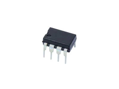
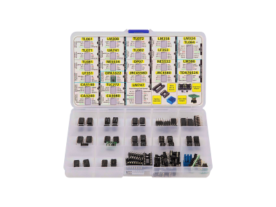
Below is a list of some common OpAmps. The same OpAmp could be made by different manufacturers with some variation in the specs. The specs in the table below are only valid for the manufacturer listed. If you're considering a chip from a different manufacturer, it is recommended that check the datasheet to see if the specs are different.
For single supply applications converting lower voltages (e.g., 5V to 3.3V), the MCP6002 or TLV2462 are good choices because they are rail-to-rail. For dual supply higher voltage applications above 5V (e.g., ±10V, ±12V, ±15V, or higher), the LM358, RC4558, TL072, or NE5532 are good choices. For low power battery applications, the LMV358A is recommended. For high speed applications, the MCP6022 and NE5532 have a large bandwidth of 10MHz.
| Part | Function | Manufacturer | In/Out | Supply Voltage |
Gain Bandwidth GBw |
Datasheet |
|---|---|---|---|---|---|---|
| LM358 |
Industry Standard
Dual OpAmp |
Texas Instruments
Product Page |
Bipolar |
Single Supply:
3V to 32V Dual Supply: ±1.5V to ±16V |
1.2MHz |
LM358 DS (PDF) |
| LMV358A |
Low Voltage
Rail-to-Rail Dual OpAmp |
Texas Instruments
Product Page |
CMOS
Rail-to-Rail |
(V+) - (V-) =
2.5V to 5.5V (±0.9V to ±2.75V) |
1.2MHz |
LMV358A DS (PDF) |
| LM741 |
General Purpose
Single OpAmp |
Texas Instruments
Product Page |
Bipolar
Max Input: ±15V |
Min: ±10V
Nominal: ±15V Max: ±22V |
1.5MHz |
LM741 DS (PDF) |
| RC4558 |
General Purpose
Dual OpAmp |
Texas Instruments
Product Page |
Bipolar
Max Input: ±15V |
Min: -18V
Max: +18V |
3MHz |
RC4558 DS (PDF) |
| LM747 |
General Purpose
Dual OpAmp |
Texas Instruments
Product Page |
Bipolar |
Min: +10V
Max: +44V |
1.5MHz |
LM747 DS (PDF) |
| MCP6002 | Low-Power General Purpose Dual OpAmp |
Microchip
Product Page |
CMOS
Single Supply Rail-to-Rail |
Min: +1.8V
Max: +6.0V |
1MHz |
MCP6002 DS (PDF) |
| MCP6022 |
Wide Bandwidth
Dual OpAmp |
Microchip
Product Page |
CMOS
Single Supply Rail-to-Rail |
Min: +2.5V
Max: +5.5V |
10MHz |
MCP6022 DS (PDF) |
| TL071 |
Low Noise FET
Single OpAmp |
Texas Instruments
Product Page |
FET |
±2.25 V to ±20 V,
4.5 V to 40 V |
3MHz |
TL07xx DS (PDF) |
| TL072 |
Low Noise FET
Dual OpAmp |
Texas Instruments
TL072 Product Page |
FET |
±2.25 V to ±20 V,
4.5 V to 40 V |
3MHz |
TL07xx DS (PDF) |
| TLV2462 |
Low Power
Dual OpAmp |
Texas Instruments
Product Page |
Bipolar
Rail-to-Rail |
Single Supply:
2.7V to 6V Dual Supply: ±1.3V to ±3V |
6.4MHz |
TLV2462 DS (PDF) |
| NE5532 |
Low Noise
High Performance Dual OpAmp |
Texas Instruments
Product Page |
Bipolar
Rail-to-Rail |
Max: ±22V | 10MHz |
NE5532 DS (PDF) |
| OP07 |
Precision
Single OpAmp |
Texas Instruments
Product Page |
Bipolar
No Rail-to-Rail |
Min: ±3.0V
Max: ±18V |
0.6MHz |
OP07 DS (PDF) |
Conclusion
Understanding how to interface analog signals so they are compatible with the range of an ADC is an important aspect of data acquisition. This article covered how to attenuate low frequency signals with a simple resistor voltage divider. For higher frequency signals, an OpAmp buffer can provide low impedance for the ADC. For negative voltages a DC bias can be used to shift the voltage by a constant amount to make it positive. Finally, a more flexible front-end design was given to allow adjusting the gain and offset of the signal.
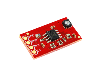
For very small signals an Instrumentation Amplifier (INAAn Instrumentation Amplifier (INA) is a type of differential amplifier in an IC that increases the disparity between its two inputs for amplifying a signal in measurements and test equipment.) would have better performance than the general purpose OpAmps used in this article. Instrumentation amplifiers are similar to basic OpAmps in the difference configuration by magnifying the difference between their positive and negative inputs, but instrumentation amplifiers have buffered inputs giving superior performance. You can construct an instrumentation amplifier from three regular op amps, but its better to use a special purpose instrumentation amplifier IC that includes accurately matched resistors needed for precision.



(0) Comments
Sign in to leave a comment
Sign In